Quantcast
Channel: dreamlayers
Viewing all 120 articles
Browse latest View live

RCA RC3000A disassembly and USB boot enabling

$
0
0
The RCA RC3000A is a small boombox with MP3 playback and recording. There is 512M flash, support for SD cards and USB storage devices, an FM radio and line in. Opening it up is kind of difficult due to plastic clips at the inner ring, around the hole. I finally got it open by applying force at the thinnest part at the front. Note how the front and speakers are attached to the top with screws, so only the bottom black part is removed.

Here's a closeup of the main board. There isn't much to see, because it is obscured by copper shielding foil and a speaker assembly.

More can be seen after removing the foil and speaker assembly. However, it's not very interesting. That's just the data flash and 2 MB of SDRAM. The SoC running it all must be hiding on the other side.

Detaching the circuit board is easy. However, the SoC is still hidden behind the LCD support.


After carefully removing the LCD support, I can see that the SoC is the Telechips TCC760. The datasheet is available!

Here's the TEA5767 FM radio:

This is the CS42L51 CODEC. To the left, R59 through R60 are 47 kΩ pulldown resistors which set the TCC760 BM (boot mode) bits to 000, meaning NOR boot without encryption. Making the right side of R60 high at reset time will change BM to 010 and select USB boot instead.

This can also be done on the other side. The capacitor pin closest to the speaker connector is +2.5V and the bottom short trace near the corner of the foil is BM1. I'm using a resistor rather than a short because the same pin is used for LRCLK for the CODEC. Yeah, it's messy, but it's temporary. I'd like to install a switch after I figure out how to run code.

Here's what shows up in Device Manager:

It might be possible to use the Rockbox tcctool program to upload code. A single one line change adding the device to the device list enables uploading, but I have not been able to confirm that any uploaded code actually runs.

The USB device ID is supported by the TeleChips firmware download driver vtcdrv.sys found in iAUDIO_COWON_D3_Upgrade_V4.53GL. There is also a VtcUsbPort.dll in the upgrader. Using these would require reverse-engineering the API. I'm hoping a simple change to tcctool will make this work.

Telechips TCC76x USB boot

$
0
0
In my previous post I opened up my RCA RC3000A and enabled USB boot on the Telechips TCC760 SoC. I'm now able to run code on it. The USB boot mode is a bit different than on later Telechips devices which are supported by the Rockbox tcctool utility. The last parameter is not the SDCFG register value, but the start address. Here is a bit of information about the USB boot mode.

All communication is in 64 byte packets. The first packet contains parameters for the USB loader routine. It must be 64 bytes, but all that matters is the first four 32-bit words:
  1. Must be 0xF0000000. If it does not match, the loader will try to use the next packet as the parameter packet, and so on, repeating. 
  2. The number of data packets, or in other words, total data size divided by 64. The loader will receive this number of 64 byte data packets after the parameter packet, and store them sequentially in memory.
  3. The destination address. The loader will store the first data packet starting at this address and store other data packets after it. The loader has no capability for performing the special actions needed to write to flash, so this must be RAM.
  4. The start address. Once the loader has received the specified number of data packets, it will jump to this address.
Note that since SDCFG is not configured, the SDRAM cannot be used and the upload should be to SRAM. The SRAM is 64 kilobytes from 0x30000000 to 0x3000FFFF, and it's also mapped to appear at 0x00000000 to 0x0000FFFF. The boot ROM is 4 kilobytes and copied to the start of SRAM, and it must not be overwritten while it is running there. You can start code at 0x00001000 or 0x30001000. The following tcctool entry can be used:

{"rc3000a",  "RCA RC3000A",                     0xb001, 0x00001000, 0x00001000 },

ROM dumping via the sound card

$
0
0
Once I got code running on the RCA RC3000A, the first task was dumping the TCC760 boot ROM and the SST39VF1601 firmware flash. The resistor I soldered for entering USB boot mode provided a convenient connection point for GPIO_B[22]. The chip runs at 2.5V, and that voltage should not be too high for line in. I carefully used an alligator clip to connect it to the tip of a 1/8" plug:

I transferred data serially using a simple ARM assembler program. Zeroes are a short pulse and ones are longer pulses. There is a short pause between bits, and a longer pause between bytes. Here is an example of 11000101 binary. I sent the least significant bit first because right shifts conveniently move it into the carry flag.
Dumping the two megabyte flash chip took an hour and a half. That's not a problem, so it's not worth investing effort in a faster communication method. For larger amounts of data, the TCC76X USB device controller would be a better choice. It seems very easy to use.

The 4KB TCC76X boot ROM has MD5 value 2579641d5be434eea15f4ec3c27a5f53. It implements USB boot mode and secure modes. However, it is not part of the normal operation of the RCA RC3000A. The boot mode is set 000, and execution starts from the SST39VF1601 firmware flash.

The 2MB firmware flash has MD5 value 89ae93fedd7fc5dff0f118aebdd4c7b6. Text strings identify it as "Thomson D100", "V2.20" and "2006.07.13". Apparently unused space with 0xFF bytes starts at 0x92E00, though there is a small chunk used at 0xFE000-0xFE0B2. This means there should be plenty of space for adding a second firmware for dual boot.

Mercury ME-DPF24MG digital photo frame reverse engineering

$
0
0
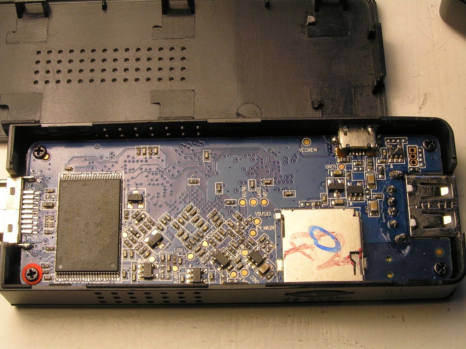
I got two Mercury ME-DPF24MG digital photo frames at the Leamington Zellers liquidation sale at 70% and 80% off the yellow tag price. They're nice 2.4" photo frames with a 320x240 LCD, rechargeable battery, a magnetic back, and a leg for standing the frame up on a desk. Some reverse engineering has already been done by others, but it's incomplete and the frame cannot be used as USB controlled display yet. The frame is also similar to the Technaxx Magno, which has been investigated more thoroughly but still cannot be used as a display.

Basic information


The frame has 4 megabytes of flash memory. The manual claims "32 MB", but I guess they mean 32 megabits. Phack from st2205tool-1.4.3 does a check for the amount of memory, and quits with "Expected response 8 on cmd 1, got 0x1f!" because the frame reports more memory than expected. Here is the external memory map, in terms of 32 kilobyte (0x8000 size) pages:

0x000-0x07F flash, starting with firmware in pages 0 and 1.
0x080-0x2FF unused
0x300-0x37F LCD
0x380-0x3FF 4 pages repeating, similar to firmware
0x400- address space repeats, probably because bank register ignores bits

The area at 0x380 seems to contain a firmware for a different photo frame. The menus are smaller than in the true firmware, implying it is for a lower resolution. Maybe it is ROM inside the chip? I did not investigate that area further.

The read command adds two to the low byte of the page number. As a result, a normal read starts right after the firmware. I dumped the firmware by reading in page 0xFE, because when firmware adds 2 to that number, it gets 0. I used 0xFE, not 0xFFFFFFFE because the firmware only adds 2 to the least significant byte of the page number.

The chip is probably a Sitronix ST2203U. It is definitely not a ST2205U because the DMA controller is different. I wasn't able to find a full User's Manual for that chip, but the ST2205U and ST2202U manuals are helpful. RAM is at 0x80-0x880 internal addresses, meaning there is only 2 kilobytes.

The LCD controller is unknown, and probably similar to Ilitek ILI9325C. The command number is 16 bit, with the most significant byte first, and coordinates are input the same way.  To talk to the LCD, set DRR to $300, send commands to $8000 and send data to $C000. Here is a sequence for setting a rectangle: C=$20, D=Y1, C=$51, D=Y1, C=$51, D=Y2, C=$21, D=X1, C=$52 D=X1, C=$53, D=X2, C=$22, followed by data with 3 bytes per pixel. This is untested.


USB Commands


Like other photo frames using Sitronix chips, the frame acts as a USB mass storage device but only responds to reads and writes to specific locations. The locations are the same as with other frames:

Write commands at 0x6200, which is SCSI sector $31, or '1'.
Write data to 0x6600, which is SCSI sector $33 or '3'.
Read data from 0xb000, which is SCSI sector $58 or 'X'

Reads from other locations start from a location in flash with "SITRONIX CORP.", which phack uses to verify the presence of a photo frame. Data writes only matter when a command has been sent, and until that command has consumed the amount of data it expects. It should be possible to split data reads and writes into multiple accesses all starting at that location. They must not be split into multiple sequential accesses because only the first chunk would go to the right location.

Commands use the first 16 bytes written to 0x6200. The first byte is the command number and the rest can be parameters. I will call the command number P0, with the parameters starting at P1. Not all commands have parameters. In some cases P1-P4 can be thought of as a page address in big endian format, with 0x8000 byte pages and the high bit being a flag used for firmware updates. Some commands return data which can be read from 0xb000 afterwards.

Here are the commands:

1: Get flash size

No parameters

Return size: 1
R0 = flash size, 0x1F with this photo frame

2: Return 32 bit checksum of flash bank

P1 : If bit 7 is high: add 6 to P4,but don't carry over to P3
P3 : for DRRH
P4 : for DRRL
2 is always added to P4 and carried over to P3. As a result 0x80000000 will checksum page 8, when it probably should be working on page 6. A firmware upgrade can be checksummed via pages 4 and

Return size: 4
R0-R3 = big endian 32 bit sum of all bytes in page

3: Write to flash

P1 : If bit 7 is high DRRL=P4+6, DRRH=0 ignoring P3. Bit 0 of byte $97 is also set. When USB is disconnected, code running in RAM copies pages 6, 7 to pages 0, 1, and then restarts the photo frame. If bit 7 is low, DRRL=P4+2 and DRRH=P3
P3 : for DRRH
P4 : for DRRL
P5 to P8 = amount to write in big endian format

No data is returned.

This function should be followed by a write of the data to 0x6600.

This function can be used to directly write to the firmware pages, but that would probably be dangerous because it could erase code that was running. The firmware update function via bit 7 of P1 should be used instead. It overwrites most of the second photo with the firmware. Note that writes to pages 6 and 7 done this way don't immediately accomplish anything special. One can read or checksum the pages to verify they were written correctly, and otherwise continue to use the USB interface. This gives you a chance to recover if there was a problem with the write. USB disconnection is the point of no return. I always did it with the power switch in the on position, so the update can continue on battery power. I don't know if having the switch in the off position might allow one to prevent an update. That or running out of battery power might be dangerous, if the update is begun but not completed.

The first 0x4000 bytes of the flash are protected on both frames. I see no code preventing writes there, so the protection must be set up in the flash chip. This is probably an attempt to avoid bricking the device, but it does not actually protect you.

4: Set read pointer

P3 = DRRH
P4 + 2 = DRRL. The add isn't carried over to DRRH.

Data is returned from $8000, according to the selected bank.

Note that there is no length parameter here. Read length comes from transfer length in READ(10) SCSI commands. This only sets a pointer which is then incremented by following reads. However, it does not wrap properly, so the second page will actually read from $0000-$7FFF, dumping the RAM, which is useful. For flash dumping, use this function before every page.

The same read pointer and data sending code is used for other commands which return data to the host. Those commands set the pointer to a location in RAM where they wrote their reply.

5: Get LCD size and BPP

No parameters

Return size: 5
R0 = high byte of width
R1 = low byte of width
R2 = high byte of height
R3 = low byte of height
R4 = bits per pixel + $80

6: Set clock

P1 = high byte of year
P2 = low byte of year
P3 = month
P4 = day in month
P5 = hours
P6 = minutes

There seems to be no way to set seconds via this interface, and the resulting seconds value is unpredictable. The user interface on the device allows setting of seconds.

Return size: 1
R0 = $5A

7: Get image format?

No parameters

Return size: 2
R0 = 9
R1 = 0

8: Get version

No parameters.

Return size: 3
R0 = $5A
R1 = 1
R2 = 5

Maybe the $5A just indicates success like after command 6, and the version is 1.5?

9: Display message

No parameters

No return data

This command uses the next data write to 0x6600 as the parameter. The first 9 characters are displayed on the LCD. Exactly the first 9 characters are displayed, so a shorter message should be padded with spaces. The function displaying the text displays a larger rectangle of text, but only 9 characters can be set via USB because the rest are overwritten.

Firmware structure and hacking possibilities


The firmware is in flash, from 0 to 0xFFFF. It is divided into 4 pages which get mapped into 0x4000-0x7FFF via PRRH and PRRL. Here, I will be talking about firmware pages, which are 0x4000 bytes in size.

Interrupt handlers, basic USB functionality and initialization except for the LCD is all in page 0. This page appears to be write protected on the flash chip. Everything that's needed to write to flash seems to be on page 0. The code checks for a valid signature at $100 in page 1, but it jumps to other pages anyways, so this doesn't protect you. It also doesn't protect you if calls to other pages hang or don't provide a way to get to USB mode.

The USB interrupt handler takes care of USB, the mass storage protocol and SCSI commands. The USB loop in main code deals with written commands and data, and sends data in response to reads. The code used to hack other photo frames goes in the USB interrupt handler. Both the USB interrupt handler and USB loop are on page 0, meaning they cannot be altered unless the page is somehow unlocked. Some commands run code on other pages, so they offer a way for running some new code.

Interrupt hooks

Interrupt handlers including the USB interrupt handler call subroutines in memory at $780 to $80C, with 14 bytes available for each routine. That is sufficient to set IRR to remap $4000-$4FFF, call a subroutine in a different firmware page, and jump to code $81A which resets IRR to 0. The calling of these routines are enabled by bit 7 of the byte at $8F. The RAM is set up to call subroutines at $4200 to $42A0 in firmware page 2, but those are only RTS instructions. Hooking might not ever be enabled normally, but it seems ready to enable. The USB interrupt hook at $78E is called after the main USB interrupt code

Hacking options

Due to page 0 being locked, there are several options:
  1. Add code to one of the commands using another page.
  2. Write code which interacts with the USB interrupt handler instead of the main USB loop.
  3. Disable interrupts and interact with the USB hardware directly.
  4. Use the USB interrupt hook.
  5. Use IRR to handle interrupts in other pages.
  6. Unlock page 0. This may involve uploading code and running it while applying a high voltage to some pin(s) of the flash chip.
I think option 1 is a good start, but other options are better eventual solutions.

Bank switching

For understanding the firmware, it is important to understand the function at $820. It is used for calling a function in another firmware bank. The function runs from RAM so it can continue through the bank switch. The call is followed by 4 bytes of parameters, and the function returns to the instruction following those two bytes. The bytes are: DRRL, DRRH, low byte of address, high byte of address. The address is the function address minus one, because the function is accessed via an RTS instruction.

There is another similar function which instead copies $200 bytes of code code to $520 and jumps there. It is used to call functions which write to flash. It uses the byte at $99 as the low byte of the source address and $9A as the high byte. There are no parameter bytes after the function call.

The DMA controller

It is also important to understand the DMA controller, because it is used often. It is more like the ST2202U than the ST2205U. Registers are:

$36 DMRL : source bank low byte
$37 DMRH : source bank high byte
$28 DMSL : source address low byte
$29 DMSH : source address high byte

$34 DRRL : destination bank low byte
$35 DRRH : destination bank high byte
$2A DMDL : destination address low byte
$2B DMDH : destination address high byte

$2C DCNTL : counter low byte, DMA trigger
$2D DCNTH : counter high byte

When reading for DMA, the DMR registers determine mapping of $8000-$FFFF. When writing, that mapping is determined by the DRR registers, like when the CPU accesses those locations. DMA can also access internal RAM. The bank registers are irrelevant then, because that address range is not banked. After a write to DCNTL, DMA starts and the CPU waits until it completes. DMA is used by interrupt code for some USB transfers and only DRRL and DRRH are saved, so interrupts need to be disabled before setting other registers. They can be re-enabled immediately after the write to DCNTL.

Running code on the Mercury ME-DPF24MG digital photo frame

$
0
0
In my previous post, I reported reverse engineering findings about the Mercury ME-DPF24MG digital photo frame. Once I figured out the most important things, it was time to start running custom code on the frame.

If firmware page 0 was writable, I would have just flashed a modified version of the code used for other Sitronix frames. Instead, I extended the "get version" command to enable displaying the USB DMA buffer for data sent by the host, and running code there. The command is parsed at flash offset $A40B, which is at $640B in firmware page 2. At that point code has access to the first 16 bytes of the sector at $381, and the last 64 bytes of the sector in the DMA buffer at $200. I used the first 4 parameter bytes at $382-$385 to trigger my code. Here is an example of the display function:


I displayed the text by calling the same function used by the message command. This is not practically useful for displaying messages, but it can confirm that my code works, and that data in the USB DMA buffer can be used.

(After the first 64 bytes, you see the DMA buffer for data being sent to the host, which starts with USBS because it is a USB mass storage status reply. The green and pink corruption outside is because the firmware upgrade code overwrites the second picture and pictures are stored in a compressed format. To prevent overwriting the code doing the firmware upgrade, the new firmware is first written there, and then copied to its final position using code copied to RAM.)

Then it was time to run code. It worked, but 64 bytes isn't much space. It wasn't even enough for the LCD set window code. At $580-$67F there is 512 bytes of RAM where flash writing procedures are copied. Since code is always copied there immediately before being executed, that area is free when not writing to flash. I wrote a small program which copied part of the USB DMA buffer to that free area. Then I used this code appended with small chunks of a longer program to assemble a longer program at $580.

Finally, this allowed me to display images. I wrote code which interacts with the USB interrupt handler to read packets sent to the data port. This is very simple. I just had to deal with a few flags and call one function after I received a packet. For faster performance, it should be possible to use polling for everything except the start and end of a packet.

Probing the device using code


The ability to run code and dump RAM also allowed me to probe the device and discover information about its hardware. By looking at flash ID bytes and the Common Flash Interface (CFI), I found that the chip is an Eon EN29LV320B in bottom boot configuration. It reports that the first two sectors are protected, but I don't know if that's due to a protection setting stored in flash or a result the WP#/ACC pin, which protects the first two sectors when low. I suspect it's due to the pin. Maybe it's connected to a GPIO pin? I also probed the LCD controller and found that it is the Ilitek IL9320.

Port A is connected to the buttons, with bits being normally high and going low when the button is pressed:
PA & 1 = left
PA & 2 = pause
PA & 4 = right
PA & 8 = menu
The slide switch seems to simply cut power, so there is no way to read it. The pause button is read at startup, changing program flow. It might be for entering a recovery mode, not calling photo frame code and immediately going into USB mode.

This is still a work in progress and I'm not releasing any code now. If you want some code, feel free to ask.

Enable volume keys in Flash Player using a hotkey program

$
0
0
Flash Player running in Firefox in Windows 7 steals keyboard events when focused. This is a well known bug that has been around for a while and isn't getting fixed. There are many Firefox and Flash bug reports on the issue. It should probably be considered a Flash bug, not a Firefox bug.

This affects all Firefox keyboard shortcuts, such as Control+Tab for switching to the next tab. It also affects some keys that Windows normally handles, such as volume up, volume down, and mute. Fortunately, it doesn't affect keys handled by HoeKey, a hotkey program. This means the problem with volume keys can be fixed by handling volume keys via HoeKey, instead of directly through Windows. Here is what needs to be added to the HoeKey configuration file:

173=Msg|Progman|793|0|524288 ; mute
174=Msg|Progman|793|0|589824 ; vol down
175=Msg|Progman|793|0|655360 ; vol up


I expect other hotkey programs could do the same thing. I like HoeKey because it uses minimal system resources, it works perfectly, and is free.

Integrated heat spreader thermal contact failure

$
0
0
I recently upgraded an old PC to a Manchester socket 939 Athlon 4200+. After booting into Stresslinux, I ran mprime (the Linux version of Prime95) to check stability and temperatures. I didn't encounter any errors, but after a few minutes, core temperatures rose past 70, and approached 80. That's bad in general and especially bad for that CPU, so I had to cut power.

After removing the heat sink, the paste application seemed fine. I tried applying paste several times, and even got some new Zalman ZM-STG2 paste, but nothing helped. I couldn't even get anything as good as the first result.

Eventually I found some message board posts about decapping, the thermal paste below the CPU integrated heat spreader (lid), and how that paste can fail. The fact that the heat sink wasn't even warm when the CPU cores approached 80, and the paste between the heat spreader and CPU seemed fine afterwards made this seem like a probable explanation.

I first attempted to cut off the integrated heat spreader (IHS) with a utility knife. This didn't work because the blade was too thick and it couldn't fit into the narrow gap between the CPU circuit board and IHS. Then I pried apart a disposable razor and got one of the blades out. It's very thin and sharp, and it fit into the gap and cut nicely. The only difficulty was that it's also highly flexible, so it can cut the circuit board. Here are pictures of the decapped CPU:


The black material that was holding the IHS is like rubber. Note that it wasn't providing a hermetic seal; there is a gap on the left of the CPU. The brown material is remnants of brasso which I used to try to lap the IHS before. The IHS was definitely slightly concave, but that wasn't the problem. The grey thermal paste was entirely dry and kind of like silicone rubber, but much easier to remove. My theory is that it works fine even when dry, and that problems happen due to the force used to separate the heat sink from the IHS. The black rubber holding the IHS allows some movement. If the dry thermal paste inside breaks apart due to that, it can't re-establish good contact.

I didn't want to run the CPU decapped because that would require modifying the motherboard, and maybe the heat sink retention. The plastic frame surrounding the socket prevents the heat sink from getting low enough to make good contact with the chip, and even if that was cut away, I'm not sure if the heat sink retention would provide enough force when the heat sink sits lower. Also, the IHS seems to be plated copper, and it might actually help with heat transfer to the stock aluminum heat sink. I just shaved down the black rubber a bit, cleaned off old paste, added new paste, and reassembled without attaching the IHS to the CPU.

After all this, running mprime on both cores resulted in temperatures of 45°C and below. This was with the stock cooler for an Athlon 64+ 3500 Newcastle (also 89W TDP) and Zalman ZM-STG2 paste.

A DIMM which won't work with any other DIMMs in the same channel

$
0
0
Since I first got it, I used my Gigabyte GA-P35-DS3R motherboard with 2 GB of DDR2 RAM. This was more than enough at first, but now it results in too much disk access even when only running KDE and Firefox.

The old RAM is an OCZ2G8002GK DDR2-800 OCZ Gold 2*1GB 5-5-5-15 kit consisting of two OCZ28001G modules. I was running it at stock speeds and voltages, and it seemed perfectly stable, never producing any errors in tests. I concluded that 4GB would probably be enough, but I chose to upgrade using 2*2GB for two reasons: I would have 4GB even if I can't get the kits working together, and it's always better to have more memory than you think you need. I found a really good deal on eBay for OCZ2P8004GK DDR2-800 OCZ Platinum 2*2GB, consisting of two OCZ2P8002G modules.

When I put in the new RAM together with the old RAM, I got a hang at the initial graphical BIOS screen, but I could boot if I only put in the new RAM. At first, this seemed like a compatibility problem, maybe because the old RAM was required 1.8V and the new RAM required 2.1V.  I had forgotten about OCZ Platinum requiring 2.1V, and that requirement wasn't stated anywhere on the eBay item page or the labels on RAM photos. I became skeptical when I saw that the old and new kits both worked alone at 5-5-5-15 timings, at either normal voltage or 2.1V. They only failed to work together.

Then I tried relaxing various primary and secondary timings and reducing the frequency. It seems the OCZ28001G modules couldn't handle CL6, but I could relax all the other timings. Nothing helped. In most cases, my computer would power off and back on twice and then hang. That seemed to be the motherboard's attempt to switch to more conservative settings. I assume it is meant to recover from a failed overclock, but it never managed to recover from this. I would have to remove a DIMM to get into BIOS setup and change settings for another attempt. Early on in this process I removed the hard drive so it doesn't get subjected to all these power cycles. Eventually I was forced to give up because I couldn't imagine what else I could change.

I tried another experiment, putting the old RAM in the slots closest to the CPU, and the new RAM in the slots further away. The intention was to put the old RAM in one channel and the new RAM in another channel, in case they were incompatible in the same channel. This configuration allowed me to boot, but caused lots Memtest86+ errors past 4 GB. According to DMI data, this address was in the middle of one of the new DIMMs. I didn't conclude anything based on this, because I didn't know if the configuration was supposed to work, and because it was weird to see errors start in the middle of a DIMM.

Later, I was inspired to try yet another experiment: two DIMMs in one channel, with nothing in the other channel. This would allow more possibilities with only 4 DIMMs. I found that one of the DIMMs wouldn't work with any other DIMM in the same channel, but the other DIMMs would work together. This finally made it seem like one DIMM is defective.

After getting a new G.Skill F2-6400CL5D-4GBPQ set, the suspect DIMM wouldn't work with either of those in the same channel, but the other OCZ2P8002G DIMM worked fine as part of a 2*2+1*1 GB DDR2-800 5-5-5-15 configuration with one of the new G.Skill DIMMs. This seems to confirm that one OCZ2P8002G DIMM is defective.

It's surprising that a DIMM can be bad in a way that it passes tests if alone in a channel but fails when there is another DIMM in the channel. However, it makes sense. Diagnostic programs can only tell you if the memory subsystem of that computer is reliably storing and retrieving data. They can't tell you if a DIMM is meeting its electronic specifications.

GA-P35-DS3R fan control

$
0
0
The Gigabyte GA-P35-DS3R motherboard has a IT8718F chip. It can control the speed of 3 fans via PWM and monitor the speed of 5 fans. The chip also has 3 thermal sensor inputs, which can be read by software. The SmartGuardian feature allows any thermal sensor input to be used to automatically control any fan without software intervention. Fan speeds can also be controlled from software. A PDF datasheet is available.

The BIOS has options to enable CPU fan speed control, and to use voltage or PWM to control the fan. I'm using voltage. The stock Q6600 fan has a 4 pin connector and supports PWM, but PWM causes noise. Voltage can control the speed just as well without the noise.

The BIOS programs the SmartGuardian feature to control CPU fan speed, but it doesn't provide any options for changing that configuration. Both Linux and SpeedFan support the IT8718F chip, but neither can program the SmartGuardian feature. SpeedFan only has an option in the Advanced tab to switch a fan from SmartGuardian to software control, which allows SpeedFan to control its speed. At least for the second PWM output, SpeedFan may not properly re-enable SmartGuardian.

An 8718fans program allows changing of SmartGuardian and other fan-related settings in the chip. It also allows viewing of current settings.

This GA-P35-DS3L information seems similar or identical to the GA-P35-DS3R. CPU fan speed is measured via the first fan sensor, and controlled via the first PWM output. That page claims that the first PWM output controls CPU fan voltage and the third output controls CPU fan PWM, which I didn't test. The second fan output controls voltage on SYS_FAN2, the 4 pin fan connector near the DIMMs and 24 pin power connector.

The BIOS sets up CPU fan control by using the second temperature sensor to control the first PWM output. This is a sensor at the CPU, but not one of the internal core temperature sensors that can be seen in programs like Core Temp. The IT8718F chip cannot use such sensors, because they can only be read by software running on the CPU. The second sensor measures temperatures which are about 10°C colder than the cores. According to 8718fans, full fan speed would be reached at 66°C, which probably corresponds to core temperatures near 76°C.

The BIOS also sets up sensor one to control PWM output two with the same settings. This is probably not reasonable for a case fan, because sensor one isn't at a particularly hot location. Its normal temperature is near 40°C, and if it reached 66°C, hotter areas would overheat.

The IT8718F SmartGuardian algorithm uses a slope, essentially just setting fan speed based on a linear relationship with temperature with some smoothing features. This means temperature depends on load, rather than being controlled to a particular level. If a certain fan speed corresponds to a certain temperature at a certain CPU load and CPU load increases, temperature increases until a new equilibrium is found, with a higher temperature and higher fan speed.

I'm now using SpeedFan to control a case fan, but still letting SmartGuardian control the CPU fan. Maybe I will inject some code into the MBR or elsewhere to set up SmartGuardian for the case fan, because I perfer not depending on an application for fan speed control.

Booting GRUB from a logical drive via the extended partition

$
0
0
The master boot record (MBR) contains code which is loaded at boot time, and a table which can list up to 4 partitions. Any data partitions created here are called primary partitions, and booting from them should be possible. One of those partitions can instead be an extended partition, which contains the same type of table, with up to 4 partitions. Partitions inside the extended partition are called logical drives, and it may not be possible to boot from those.

I installed Linux on a logical drive. Due to known problems installing Windows service packs when GRUB is in the MBR, I refused to put GRUB there and instead put it in the logical drive containing Linux. GRUB was normally loaded by the Windows 7 bootloader.

Now I wanted to boot directly into GRUB, so I can use it to hide and unhide partitions and select between two versions of Windows. Making just the logical drive with Linux active did not work. The result was as if there is no active partition. It is possible to make the extended partition active, but grub-install refuses to install there, probably because grub-probe can't figure out the mapping for it.

I solved this by copying the code from the Linux logical drive boot sector to the first sector of the extended partition. It was simple, via "sudo dd if=linux_logical_drive_partition bs=446 count=1 of=extended_partition". The code is 446 bytes long, starting at the beginning of the sector. The rest of the destination sector contains information about partitions, which must not be overwritten. It is extremely important to use the right device names here. (They will typically be something like /dev/sda5, with the logical drive having a higher number than the extended partition.) Mistakes in dd commands writing to raw disk devices can cause unrecoverable data loss.

GRUB's first stage code doesn't care from where it's loaded. However, it does contain hard-coded sector locations, and if that needs to change it would have to be copied again in the same way.

Craig CVD601 Android stick

$
0
0

I got a Craig CVD601 Android stick at the XS Cargo closing sale for $30. Android devices which are designed to be hooked up to a TV interested me, but I didn't have enough faith in the idea to actually order one. This was cheap and a good deal even compared to ordering from China, so I decided to try it out.

The device came with Android 4.1 Jelly Bean and worked, but the WiFi is terrible. At the same location, my laptop gets a good signal but the CVD601 can only occasionally connect with a terrible transfer rate. Best results were on channel 2, but even that was not usable. I created an access point on my laptop, but that's not a permanent solution.

Rooting

I quickly decided that rooting is necessary, because I don't want to keep running into obstacles where I can't do something because I don't have root access. This wasted a lot of time because various methods I tried didn't work. Some rely on security bugs which were fixed in earlier versions, or are designed to only work with particular devices. Eventually I found Cydia Impactor, which rooted the device quickly and easily. I used Impactor_0.9.14.zip, with MD5 162761dcbe0b2c0ac08cfb86dea8d715. Then I manually installed SuperSU.

After rooting, I edited /system/default.prop, removing tethering and developer_options from ro.wmt.ui.settings_remove to enable those settings. ADB access was available before, but this makes some things more convenient. I will also enable Ethernet settings when I get the USB adapter. Note that /system is normally mounted read-only, so it needs to be remounted via "mount -o remount,rw /system" before making changes. When done with  changes, use "mount -o remount,ro /system" to make it read-only again.

Reverse tethering

Reverse tethering provides better network performance than wireless, but I had too much trouble getting it started, and I don't recommend wasting time on this. First, tethering needs to be enabled. If the option is greyed out, enable USB debugging first. Then, on the Android side, the rndis0 interface needs to be reconfigured. I never got "netcfg rndis0 dhcp" working, so I had to configure manually, with ifconfig and route. Windows contains the driver but requires an INF file. I used Microsoft's template customized with USB\VID_18D1&PID_0003.

Google Play

I also decided I had to install Google Play Store, because many apps are only available there. It's possible to download APK files and then install them, but that makes things more complicated. If simply installed like any other app, Play Store runs fine at first but crashes as soon as I try to download anything. After that, it keeps crashing on startup. This is because it doesn't have permission to install apps. The solution is installing it as a system app, by copying its APK to the /system/app folder with chmod 644. The app will also crash if its version is incompatible with the version of Google Play Services that is already installed. I installed FirmwareInstall/GoogleApp/system/app/Vending.apk from cvd601_602_firmware4.1.zip available on the Craig site. Then it updated both the store and the services app to the latest version, and everything worked fine after that.

Internals and the WiFi issue

Due to the WiFi problem and my curiosity I decided to open up the device:

 Here is a closeup of the RTL8188ETV based WiFi module. It is a USB device, but with 3.3V power. You can find PDF documentation for similar devices online. The pins below and to the left connect to the antenna. Their top narrow part is spring loaded.
Here is the antenna, note the indentations from where the pins connected. The left black part of the sticker has no metal underneath, and the right part is one solid sheet of metal. Antenna and ground are shorted together, with only that little slot between them. I wonder what kind of antenna this is, and how it works. RF seems like magic sometimes.
After experimenting with various wires connected to the pins, I found I got the best results with two quarter-wavelength wires placed 90 degrees apart. Then I cut the sticker in half lengthwise and glued the parts back on 90 degrees apart. This gave me a reliable connection to the router which was good enough for the web at least, but it didn't work the next day. Then it worked again after I squeezed the device near where the pins are. Maybe the pins don't make good contact? In any case, I don't want to waste more time on this, so I'll wait until I get the USB Ethernet adapter.

Kernel source and config

The 3.0.8 Linux kernel for WM8850 is available on GitHub. It includes binary modules from WonderMedia. The configuration file can be extracted from the kernel on the device. Here is the kernel config for your convenience. The kernels in the boot image, recovery image and cvd601_602_firmware4.1.zip are identical.

Trying out a cheap Chinese 100W LED array

$
0
0
Recently I found that Chinese 100W LED arrays cost less than $5 on eBay, so I had to try one out. The LED array arrived in less than a month in a padded envelope with no other protection. This is not right, because white LEDs are static sensitive, but I guess you can't expect much for $5, and the LED works. Here's the LED at very low power:
Note how the LEDs have unequal brightness. One whole row is brighter, presumably because the dark LED in that row has greater forward leakage and a low voltage drop across it. This all looks bad, but it's normal at low power. Using higher current and a low PWM duty cycle would probably produce more uniform results, if that was needed.

The biggest heat sink I had was a Slot-A Athlon heat sink. After mounting it the first time, without paste just to check the fit, I could see light between the LED and the heat sink. There were high spots at the plastic-filled holes and slots in the LED's metal plate. I don't think the plastic was high; it seems more like the metal was distorted by punching operations. The whole thing was also warped on a larger scale. After sanding it with fine sandpaper on a piece of glass, I got a much better fit and mounted it.
Note how the LEDs have very similar brightness now at higher power. The LED is a bit dirty from Brasso, which was probably unnecessary. Fine sandpaper was good enough.

Then there was the question of how to drive the LED. I have a power supply from an old Fujitsu SMD hard drive, with -12V and +24V outputs, giving 36V, which is more than enough for the LED. I set up some primitive linear current regulation, using a 0.22 ohm resistor and Vbe of a small transistor. The transistor controlled the gate of a power MOSFET with a big heat sink. This works surprisingly well, though note that Vbe changes with temperature. It regulated the current to 2.7A and I measured 35V accross the LED.

The heat sink required some serious airflow to stay cool enough that I could keep my finger on it indefinitely near the LED. Fortunately that same SMD hard drive had two 8 cm fans, to which I added some cardboard ducting to concentrate the air. The power supply even monitors the fans, not via RPM but via thermistors which are cooled by airflow and heated by resistors.
The light coming from the LED is surprisingly hot. My fingers quickly feel burning hot within a few centimetres of the light emitting face, and heat can be felt much further away. It's not the soothing heat of an incandescent, but something more like the feeling of steam escaping from a pot. I guess that's because the infrared light from incandescent bulbs penetrates deeper than visible light.

The LED is also incredibly annoying to look at, and worse than the sun or even badly aimed HID headlights. It's totally unacceptable to have this LED even in the farthest part of my peripheral vision. At the same time, the room doesn't really feel very bright.

In the past I was thinking of retrofitting a powerful LED into a halogen torchiere which had a bad bulb socket. I didn't do it because I wasn't sure I could deal with the heat in an acceptable way. Two high speed fans are fine for experimentation, but a light I use every day should be fanless or at best have a slow speed fan. Instead I ended up fixing the torchiere, making new socket contacts from brass pluming screws.

Comparing light from the 300W halogen torchiere and the 100W LED operating at around 90W, I definitely prefer the torchiere. It makes the room seem brighter even though the LED might actually be a bit brighter. It's hard to compare brightness due to different colours and lamp positions, but I don't think this LED is capable of 9000 to 10000 lumens at 3A. The LED's colour is also somewhat weird. Colours which would normally seem close to white seem yellowish or purplish.

Overall, I'm not too impressed. The light I'm getting doesn't make me want to create a more permanent lamp or flashlight using this LED. It was fun to play with though, and certainly worth the $5.

Yellowish light seems brighter, and bright bluish light is more annoying

$
0
0
The brightness of the 100W cool white LED is confusing. After being for a while in a room illuminated by it, the room seems quite dim. Going away and coming back shows that the room is in fact very bright. A 300W halogen torchiere is probably dimmer than the LED, but the room seems brighter when lit that way, and that feeling of brightness doesn't go away.

The LED array itself seems extremely annoyingly bright. It is so bad that I can't stand it even in the farthest peripheral vision, and I will walk sideways with my back turned to it to avoid seeing it.  The effect reminds me of HID headlights, but it's even worse. It's much worse than the sun or high power halogen lights.

I'm also reminded of how brown sunglasses affect perceived brightness. Their darkened lenses obviously decrease real brightness. However, on a bright sunny day they only seem to reduce the unpleasant aspects of excessive brightness, and they can even increase perceived pleasant brightness.

This gives me some ideas. Does yellowish light trigger pleasant feelings of brightness, and does bluish light trigger unpleasant feelings of excessive brightness? Does yellowish light constrict pupils less than bluish light?

Chain booting Linux from Windows using Darwin chain0

$
0
0
EasyBCD can create a Windows boot menu entry for Linux, using GRUB installed in its partition. This copies the boot sector of the selected partition to C:\NST\nst_linux.mbr and sets up an entry to boot via that file. This works, but it can stop working if upgrades are installed in Linux and the boot sector changes. In that case, the boot sector needs to be copied to that file again. Deleting and re-creating the menu entry in EasyBCD will accomplish that.

It would be better to read the boot sector directly, but I don't think Windows supports that. Another alternative is to use a boot sector file which finds and loads the real boot sector. This approach is used when loading Mac OS X or Darwin via chain0. You can obtain a version of chain0 at C:\NST\nst_mac.mbr by setting up a Mac OS X MBR boot entry in EasyBCD. The version I have has an MD5 value of cfca64f400ef99e89b51e59bcb697137. I patched it to search for the Linux partition instead of OS X and used that version as nst_linux.mbr:

C:\NST>fc /b nst_mac.mbr nst_linux.mbr
Comparing files nst_mac.mbr and NST_LINUX.MBR
0000008A: AB 83
00000090: A8 83
00000096: AF 83

It can search for three different partition types, but I only need to search for one so I set them all to 83 hex. This can successfully boot Linux from the first partition in my extended partition. If you have a more complicated setup, you may need a different version of chain0 with a fix for accessing other partitions in the extended partition.

If nRF24L01 modules don't work, add decoupling capacitors

$
0
0
I got two nRF24L01+ modules and tried to establish communication between the MSP430 and Stellaris LaunchPads. SPI communication worked, and I was able to read and write registers, but all attempts at wireless communication were a total failure. I even tried a kind of promiscuous mode, where I was getting data, but it all seemed to be garbage with no trace of the packets I was transmitting. Something was definitely being transmitted according to the chip's received power detector, though it was suspiciously spread out onto adjacent channels.

After wasting a few hours trying to figure out what was wrong with the software and finally taking a break, I got the idea to try adding bypass capacitors. They made everything work. The modules do have C8 and C9 which are supposed to be 1 nF and 10 nF respectively, but those are clearly not enough when the power supply wires are long. I just used some small electrolytic capacitors I had around, 56 µF on one module and 33 µF on another. Tantalum capacitors would be a better choice because of their smaller size and good high frequency performance.


Trying out a mini logic analyzer

$
0
0
I just got a small and inexpensive logic analyzer from dx.com. Basically, it contains a CY7C68013A microcontroller and 74HC245 buffer chip, and you can upload firmware which makes it into a logic analyzer.

I used sigrok PulseView. First I tried it in Windows. It's easy to install the driver using the included Zadig executable. After that, PulseView tended to crash on startup if the logic analyzer was connected. I only got it to run a few times. Also, it seemed to lock up sometimes when capturing for a second or third time. I expect this is due to bugs in the Windows version of PulseView, and not due to a problem with the hardware.

Here's a decode of a NEC protocol IR remote. I couldn't get it to work at the default 20 kHz sample rate, even though that should have been fast enough. It worked at 100 kHz.
Here's some 9600 baud serial communication. This is also at 100 kHz. It also worked at 20 kHz sampling if I set the decoder baud rate to 10000. Problems with 20 kHz are understandable though, because it's just a bit over twice the baud rate.
After this I rebooted into Linux because the Windows problems were getting too annoying. Installing sigrok was easy, because a Ubuntu package was available. I didn't have any problems in Linux. Here's some SPI. The Stellaris LaunchPad is communicating with an nRF24L01+ module and writing to some registers. This is at the maximum sample rate of 24 MHz.
As you can see, with a small piece of hardware you can order from China for $10 and some free software, you can have a 24 MHz logic analyzer which will decode protocols for you. That's truly impressive!

Music visualization using an RGB lamp

$
0
0
I wrote Winamp and Audacious music visualization plugins for my RGB lamp. The code is published on GitHub. Pitch is represented by colour, and loudness is represented by intensity. This post explains the method in detail.

The code starts with an array of FFT bin values. This is provided by the music player via its visualization plugin API. If only waveform data was available, the FFT could be computed using the FFTW library.

Each value in that array corresponds to sound intensity in a particular range of frequencies. Those ranges are all of equal width in hertz, but humans perceive pitch in a roughly logarithmic way. This means perceived pitch varies a lot between entries at the start of the array, and a little at the end of the array. This is handled by makeramps.rb. The frequency at the midpoint of each bin is mapped to pitch using the MIDI pitch formula. This allows pitch to be mapped to colour in a sort of linear way. Here's how the various FFT bins sum into the different colours:
The lowest frequency bin sums to red. Increasing frequencies sum less into red and more into green. The pitch midpoint sums into green. Then increasing frequencies sum less into green and more into blue. Finally, the highest frequency sums into blue. The code uses a single table called green_tab, with values corresponding to the fraction of the bin that is to be summed into green. Before the pitch midpoint, one minus the table value times the bin is summed into red, and after the midpoint the same is summed into blue.

Before summing, bins can be scaled based on human ear audio sensitivity at that frequency. This ensures that frequencies where the human ear is less sensitive make less of a contribution. I found an ISO 226 Equal-Loudness-Level Contour Signal script for MATLAB which can run in GNU Octave. This isn't very important though.

When summing bins, it is important to sum power, not amplitude. Summing amplitudes does not make sense, but fortunately they are easy to convert to power: just square them before summing. Afterwards, they are converted back to amplitude via square root, because they are to be used for setting PWM values.

If the output of this algorithm was used to directly set lamp brightness, there would be a lot of rapid brightness changes. I find this unpleasant, so I added some smoothing. The code calculates an exponential moving average for each colour, but with more smoothing for decreases and less smoothing for increases. The faster response to increases ensures the lamp will appear responsive to loud sounds.

After all this, the colours still did not appear to be in balance. To fix this, I calibrated using pink noise, and created scale factors for red and blue which cause white light when playing pink noise. It may be better to calibrate using music, but that would be more difficult and the resulting calibration might be biased toward the music used to calibrate it.

I'm posting about this because of how I'm satisfied with the end result. I haven't done any tweaking of this algorithm in many months, and I still really like the effect.

Recently I have been experimenting with an on-screen visualization plugin inspired by this. Each moment is displayed on a horizontal line with stereo determining horizontal position. Pitch sets colour, intensity sets brightness, and very intense sounds cause a wider area to be coloured.  Old data scrolls down. This part is still a work in progress, and I haven't published that code yet.

The earliest sunset is not on the winter solstice

$
0
0
I thought the earliest sunset occurs on the winter solstice. That's not true. As you can see here, the sun set at 5 PM for the first half of December, and started setting later after that. It will continue to rise later every day, until a plateau in early January.

Access to physical disk devices in Windows 7

$
0
0
I just noticed that PhotoViewer, the program for putting photos on the first digital photo frame I hacked, did not need to run as Administrator. It simply opens the drive using CreateFileA() and a path like "\\.\D:". I could use the same sort of path to open another USB storage device, so Windows isn't somehow recognizing the photo frame and allowing this for compatibility.

The CreateFileA documentation tells you to use a path like "\\.\PhysicalDrive1", but that only works for me if run as Administrator.

There is a difference between the two paths: "\\.\D:" is a partition and "\\.\PhysicalDrive1" is an entire drive. However, if the drive is not partitioned, the two are effectively the same.

Cygwin works the same way. The physical drive is "/dev/sdb", requiring Administrator access, and the partition is "/dev/sdb1", not requiring administrator access. The first partition exists even if the drive is not partitioned, and then it is the same as the whole drive.

Opening for writing can fail sometimes if the device is in use, but otherwise, even a non-admin user can write to sectors. I can have a FAT32 formatted USB drive open in an Explorer window and simultaneously write to sectors altering the files there. It does not work with an NTFS formatted drive, so this is not as insecure as it might seem at first.


The hard problem with porting DOSBox to Emscripten.

$
0
0
Getting DOSBox to successfully run many programs in a web browser wasn't hard, thanks to Emscripten. Improving performance was a bit harder. Here I'm going to describe the hardest problem, which still remains unsolved. Because of it, some programs cause web browsers to hang, and the interactive command prompt is unusable.

JavaScript code must return to the browser regularly. That's the only way the browser can regain control so it can update the display and handle new input. If JavaScript code doesn't return, the page or the whole browser appear to hang. The script may be producing output, but the user won't see it until the browser regains control. There isn't any function you can call to let the browser do its work. Your functions literally must return.

DOSBox emulates a PC running DOS using a mix of x86 assembly running under CPU emulation and C++ code running on the host. This can result in deeply nested calls. Here is the call stack from a program reading from the keyboard via the DOS device CON:

#0  DOSBOX_RunMachine () at dosbox.cpp:244
#1  0x000000000040e1f4 in CALLBACK_RunRealInt (intnum=22 '\026')
    at callback.cpp:106
#2  0x00000000004a1ed5 in device_CON::Read (this=0x3a2c430,
    data=0x7fffffffa15d "", size=0x7fffffffa12a) at dev_con.h:66
#3  0x00000000004a2f9b in DOS_Device::Read (this=0x3a4c1e0,
    data=0x7fffffffa15d "", size=0x7fffffffa12a) at dos_devices.cpp:67
#4  0x00000000004a73b7 in DOS_ReadFile (entry=0, data=0x7fffffffa15d "",
    amount=0x7fffffffa176) at dos_files.cpp:371
#5  0x000000000049e429 in DOS_21Handler () at dos.cpp:196
#6  0x00000000004073cf in Normal_Loop () at dosbox.cpp:135
#7  0x00000000004077bb in DOSBOX_RunMachine () at dosbox.cpp:244
#8  0x000000000040e1f4 in CALLBACK_RunRealInt (intnum=33 '!')
    at callback.cpp:106
#9  0x00000000006a8ecc in DOS_Shell::Execute (this=0x3a4c2c0,
    name=0x7fffffffbaf0 "debug", args=0x7fffffffcbe5 "") at shell_misc.cpp:492
#10 0x00000000006a0613 in DOS_Shell::DoCommand (this=0x3a4c2c0,
    line=0x7fffffffcbe5 "") at shell_cmds.cpp:153
#11 0x000000000069d96f in DOS_Shell::ParseLine (this=0x3a4c2c0,
    line=0x7fffffffcbe0 "debug") at shell.cpp:251
#12 0x000000000069ded8 in DOS_Shell::Run (this=0x3a4c2c0) at shell.cpp:329
#13 0x000000000069e8d2 in SHELL_Init () at shell.cpp:653
#14 0x00000000006978a8 in Config::StartUp (this=0x7fffffffddc0)
    at setup.cpp:853


There you can see the program running at #6. Normal_Loop() usually keeps calling the CPU emulator to run x86 code, but some instructions cause the emulator to quit, returning a value that tells Normal_Loop() to call a different function. In this case, the CPU emulator encountered int 21h, the main way to access DOS services. That is why Normal_Loop() called DOS_21Handler() at #5. After that, things are happening directly via C++ code, without CPU emulation. Then at #2, device_CON::Read() is calls int 16h (22 decimal), the BIOS interrupt for the keyboard. It calls either ah=0 or ah=10h functions, both of which wait for a key to be pressed and then return its value. The interrupt handler is implemented in x86 code, so you see DOSBOX_RunMachine() at #0. There is also a loop in device_CON::Read(), which keeps calling int 16h until it has the requested number of characters.

Such inner loops at #2 and #0 are not compatible with JavaScript. It's not possible to just keep waiting for input like that. Instead, the functions need to return, and then run again in the next iteration of the Emscripten main loop. That would involve re-establishing the entire call stack, with parameters and local variables.

Actually, my port has a shortcut. That backtrace is normal DOSBox running in Linux. My port establishes the Emscripten main loop at #7, in DOSBOX_RunMachine(). Because of that, there is no need to worry about #14 through #7. Because of this, when the running program exits, you can't get back to the DOS prompt. That's okay for now, because the interactive command prompt can't work anyways. It similarly gets stuck in a loop..

This is not impossible to fix, but I can't imagine a nice elegant fix yet. Adding code to re-establish that call stack on the next main loop iteration would be messy. It would also degrade performance. Maybe it would be possible to strip out DOS emulation and run FreeDOS instead? Currently DOSBox does not have a disk controller and relies on its DOS emulation to access files. The DOXBox-X branch adds an IDE controller.
Viewing all 120 articles
Browse latest View live